- 您现在的位置:买卖IC网 > Sheet目录2004 > LTC1747IFW#PBF (Linear Technology)IC ADC 12BIT 80MSPS 48-TSSOP
1
LTC1747
1747fa
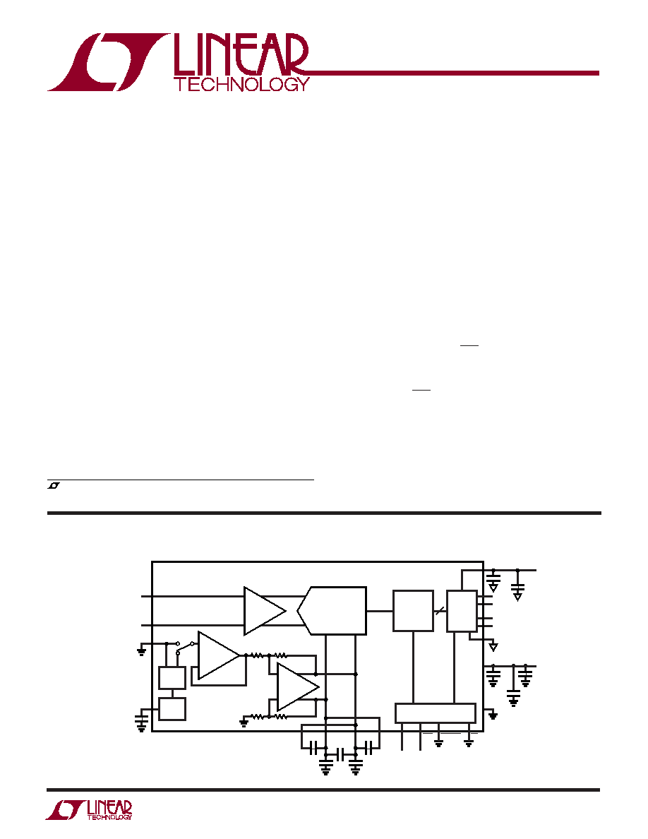
BLOCK DIAGRA
W
APPLICATIO S
U
FEATURES
DESCRIPTIO
U
12-Bit, 80Msps Low Noise ADC
s
Sample Rate: 80Msps
s
72dB SNR and 85dB SFDR (3.2V Range)
s
70.5dB SNR and 87dB SFDR (2V Range)
s
Pin Compatible with 14-Bit 80Msps LTC1748
s
No Missing Codes
s
Single 5V Supply
s
Power Dissipation: 1.4W
s
Selectable Input Ranges:
±1V or ±1.6V
s
240MHz Full Power Bandwidth S/H
s
Pin Compatible Family
25Msps: LTC1746 (14-Bit), LTC1745 (12-Bit)
50Msps: LTC1744 (14-Bit), LTC1743 (12-Bit)
65Msps: LTC1742 (14-Bit), LTC1741 (12-Bit)
80Msps: LTC1748 (14-Bit), LTC1747 (12-Bit)
s
48-Pin TSSOP Package
s
Telecommunications
s
Receivers
s
Cellular Base Stations
s
Spectrum Analysis
s
Imaging Systems
, LTC and LT are registered trademarks of Linear Technology Corporation.
The LTC
1747 is an 80Msps, sampling 12-bit A/D con-
verter designed for digitizing high frequency, wide dy-
namic range signals. Pin selectable input ranges of
±1V
and
±1.6V along with a resistor programmable mode
allow the LTC1747’s input range to be optimized for a wide
variety of applications.
The LTC1747 is perfect for demanding communications
applications with AC performance that includes 72dB
SNR and 85dB spurious free dynamic range. Ultralow jitter
of 0.15psRMS allows undersampling of IF frequencies with
excellent noise performance. DC specs include
±1.5 LSB
INL and
±0.8LSB DNL over temperature.
The digital interface is compatible with 5V, 3V, 2V and
LVDS logic systems. The ENC and ENC inputs may be
driven differentially from PECL, GTL and other low swing
logic families or from single-ended TTL or CMOS. The low
noise, high gain ENC and ENC inputs may also be driven
by a sinusoidal signal without degrading performance. A
separate output power supply can be operated from 0.5V
to 5V, making it easy to connect directly to any low voltage
DSPs or FIFOs.
The TSSOP package with a flow-through pinout simplifies
the board layout.
80Msps, 12-Bit ADC with a 2V Differential Input Range
12-BIT
PIPELINED ADC
12
S/H
AMP
±1V
DIFFERENTIAL
ANALOG INPUT
AIN
+
AIN
–
SENSE
VCM
4.7
F
DIFF AMP
REFLA
REFHB
GND
1747 BD
ENC
4.7
F
1
F1F
0.1
F
0.1
F
REFHA
REFLB
BUFFER
RANGE
SELECT
2.35VREF
CORRECTION
LOGIC AND
SHIFT
REGISTER
OUTPUT
LATCHES
CONTROL LOGIC
OVDD
VDD
OGND
0.5V
TO 5V
5V
0.1
F
1
F
1
F
1
F
D11
D0
CLKOUT
OF
ENC
DIFFERENTIAL
ENCODE INPUT
OE
MSBINV
0.1
F
发布紧急采购,3分钟左右您将得到回复。
相关PDF资料
LTC1748CFW#TRPBF
IC ADC 14BIT 80MSPS 48-TSSOP
LTC1749IFW#PBF
IC ADC 12BIT 80MSPS SMPL 48TSSOP
LTC1750IFW#PBF
IC ADC 14BIT 80MSPS SMPL 48TSSOP
LTC1799HS5#TRPBF
IC OSC SILICON 33MHZ TSOT23-5
LTC1821ACGW
IC D/A CONV 16BIT PRECISE 36SSOP
LTC1851CFW
IC ADC 12BIT 1.25MSPS 48-TSSOP
LTC1853IFW#TRPBF
IC A/D CONV 8CH 12BIT 48-TSSOP
LTC1856IG#PBF
IC ADC 16BIT 100KSPS 28-SSOP
相关代理商/技术参数
LTC1747IFW#TR
功能描述:IC ADC SMPL 12BIT 80MSPS 48TSSOP RoHS:否 类别:集成电路 (IC) >> 数据采集 - 模数转换器 系列:- 标准包装:1 系列:- 位数:14 采样率(每秒):83k 数据接口:串行,并联 转换器数目:1 功率耗散(最大):95mW 电压电源:双 ± 工作温度:0°C ~ 70°C 安装类型:通孔 封装/外壳:28-DIP(0.600",15.24mm) 供应商设备封装:28-PDIP 包装:管件 输入数目和类型:1 个单端,双极
LTC1747IFW#TRPBF
功能描述:IC ADC 12BIT 80MSPS 48-TSSOP RoHS:是 类别:集成电路 (IC) >> 数据采集 - 模数转换器 系列:- 产品培训模块:Lead (SnPb) Finish for COTS
Obsolescence Mitigation Program 标准包装:2,500 系列:- 位数:12 采样率(每秒):3M 数据接口:- 转换器数目:- 功率耗散(最大):- 电压电源:- 工作温度:- 安装类型:表面贴装 封装/外壳:SOT-23-6 供应商设备封装:SOT-23-6 包装:带卷 (TR) 输入数目和类型:-
LTC1748CFW
功能描述:IC ADC 14BIT 80MSPS 48-TSSOP RoHS:否 类别:集成电路 (IC) >> 数据采集 - 模数转换器 系列:- 标准包装:1 系列:- 位数:14 采样率(每秒):83k 数据接口:串行,并联 转换器数目:1 功率耗散(最大):95mW 电压电源:双 ± 工作温度:0°C ~ 70°C 安装类型:通孔 封装/外壳:28-DIP(0.600",15.24mm) 供应商设备封装:28-PDIP 包装:管件 输入数目和类型:1 个单端,双极
LTC1748CFW#PBF
功能描述:IC ADC 14BIT 80MSPS 48-TSSOP RoHS:是 类别:集成电路 (IC) >> 数据采集 - 模数转换器 系列:- 标准包装:1 系列:- 位数:14 采样率(每秒):83k 数据接口:串行,并联 转换器数目:1 功率耗散(最大):95mW 电压电源:双 ± 工作温度:0°C ~ 70°C 安装类型:通孔 封装/外壳:28-DIP(0.600",15.24mm) 供应商设备封装:28-PDIP 包装:管件 输入数目和类型:1 个单端,双极
LTC1748CFW#TR
功能描述:IC ADC SMPL 14BIT 80MSPS 48TSSOP RoHS:否 类别:集成电路 (IC) >> 数据采集 - 模数转换器 系列:- 标准包装:1 系列:- 位数:14 采样率(每秒):83k 数据接口:串行,并联 转换器数目:1 功率耗散(最大):95mW 电压电源:双 ± 工作温度:0°C ~ 70°C 安装类型:通孔 封装/外壳:28-DIP(0.600",15.24mm) 供应商设备封装:28-PDIP 包装:管件 输入数目和类型:1 个单端,双极
LTC1748CFW#TRPBF
功能描述:IC ADC 14BIT 80MSPS 48-TSSOP RoHS:是 类别:集成电路 (IC) >> 数据采集 - 模数转换器 系列:- 产品培训模块:Lead (SnPb) Finish for COTS
Obsolescence Mitigation Program 标准包装:2,500 系列:- 位数:12 采样率(每秒):3M 数据接口:- 转换器数目:- 功率耗散(最大):- 电压电源:- 工作温度:- 安装类型:表面贴装 封装/外壳:SOT-23-6 供应商设备封装:SOT-23-6 包装:带卷 (TR) 输入数目和类型:-
LTC1748IFW
功能描述:IC ADC SMPL 14BIT 80MSPS 48TSSOP RoHS:否 类别:集成电路 (IC) >> 数据采集 - 模数转换器 系列:- 标准包装:1 系列:- 位数:14 采样率(每秒):83k 数据接口:串行,并联 转换器数目:1 功率耗散(最大):95mW 电压电源:双 ± 工作温度:0°C ~ 70°C 安装类型:通孔 封装/外壳:28-DIP(0.600",15.24mm) 供应商设备封装:28-PDIP 包装:管件 输入数目和类型:1 个单端,双极
LTC1748IFW#PBF
功能描述:IC ADC 14BIT 80MSPS 48-TSSOP RoHS:是 类别:集成电路 (IC) >> 数据采集 - 模数转换器 系列:- 标准包装:1 系列:- 位数:14 采样率(每秒):83k 数据接口:串行,并联 转换器数目:1 功率耗散(最大):95mW 电压电源:双 ± 工作温度:0°C ~ 70°C 安装类型:通孔 封装/外壳:28-DIP(0.600",15.24mm) 供应商设备封装:28-PDIP 包装:管件 输入数目和类型:1 个单端,双极